
Packaging Technology
Changes in Package Shapes of ICs and LSI devices
1990s
1990s: Era of CSPs (chip-scale or chip-size packages) as compact packages for surface mountingProgress in the standardization of package outlines led to a shift of major production sites to the areas as South East Asia, Taiwan, and Korea. Japan focused its development efforts on CSP technology as a compact surface-mount technique that would enable mounting at even higher densities. The development of CSPs, allowing incorporation of the device functions of electronic systems in the smallest possible shape, led to still more compact information appliances (e.g. cellular phones) hitting the marketplace.
1990: Shipment of large-scale computers using the MCC, a small package with high heat-dissipation
Hitachi developed a method of mounting packages in a small form but with good heat-dissipation characteristics. The micro chip carrier (MCC) was the pioneering type of CSP. In an MCC, the LSI device is connected to a 10- to 12-mm-square mullite ceramic substrate by means of solder balls. 528 solder balls for mounting the MCC on the module board were stuck to the bottom surface in a grid pattern with a spacing of 0.45 mm, and a water-cooling system was also mounted on the board.
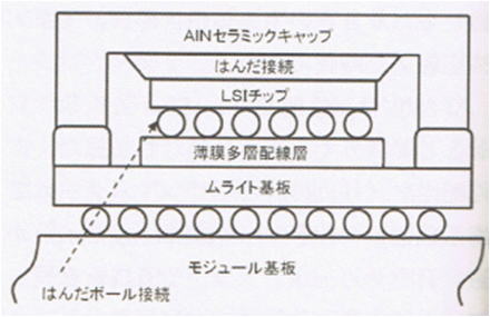
High Heat Dissipation MCC (Micro Chip Carrier) for Main-Frame Application
1991: Development of a technique for flip-chip interconnection with the resin substrate
As a replacement for costly multilayered ceramic substrates, IBM Japan Ltd. announced a technique for directly mounting LSI devices on printed-circuit boards by using flip-chip connection in January ,1991. The printed-circuit boards were made by the “build-up method”, which allows the formation of very fine wiring patterns. Reducing costs by switching the substrate material from ceramic to resin and improving performance by using copper wiring in place of tungsten wiring led this to become the basic technique for low-cost packages with high performance.
Flip-Chip Direct Mounting of LSIs on Printed Circuit Board
1991: Announcement of the adoption of an LOC structure for 16-Mbyte DRAM
After their legal battle at the ITC, TI and Hitachi advanced with a cooperative DRAM development project (the GT (Get Together) project) and announced their adoption of an LOC (lead on chip) structure for 16-Mbit DRAM in Nikkei Microdevices. This became the basic structure for subsequent DRAM packages because of its many advantages: placing the lead frame on the DRAM chip eased the handling of further reductions in chip size, adjustments to handle more parallel output bits were easy, and the package allowed high-speed transmission.
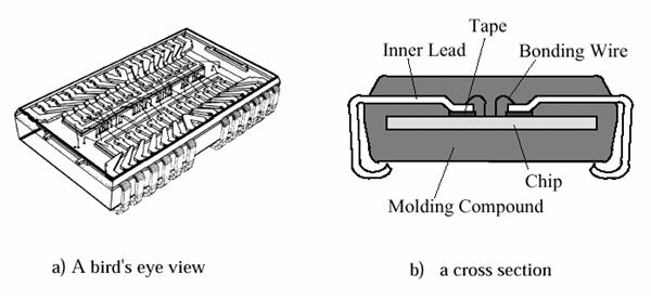
16Mbit DRAM in LOC Package
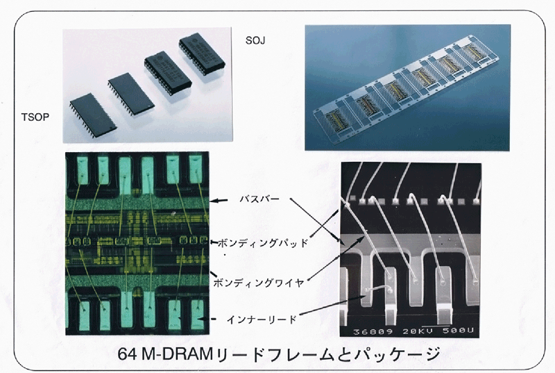
64Mbit LOC Lead Frame and Package
1992: Start of mass production of LGA-type CSPs
In 1992, Matsushita Electronics Corp. mass-produced the small LGA (land grid array), in which gold-wire stud bumps were formed on the LSI device and these were used to flip-chip connect of the device to a ceramic substrate. This package was used for the microprocessors of cellular phones.
LGA-Type CSP
1994: Development of BGA
For the COB structure of LSI devices mounted on a multilayer printed-circuit board, BGA (ball grid array) with sticking solder balls to the terminals on the bottom surface of a COB was developed. Narrowing the inter-ball pitch then led to the FBGA (fine-pitch BGA) package, which was heavily used for the LSI circuits of cellular phones.
COB with BGA (Ball Grid Array)
1994: Asserting CSP's priority over MCM
The U.S. at the time was promoting the multi chip module (MCM), in which a system was integrated by lining up multiple LSI devices on a printed-circuit board and connecting them by wire bonding. Japan presented at a SEMI session the superiority of CSP over MCM, in that CSP enabled full exploitation of device performance with smallest package outline, thus more suitable for high performance electronic system. The CSP became the focus for the subsequent global development of packages.
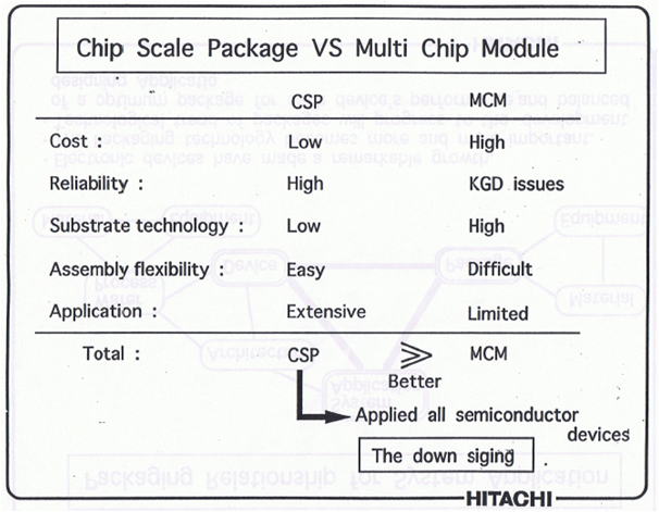
Superiority of CSP over MCM
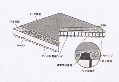
1996: Mass production of CSPs having tape substrates starts
In 1996, Sharp started mass production of a CSP which used a TAB tape substrate made of polyimide tape and having solder balls stuck to its under-surface.
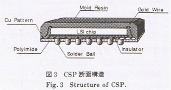
Cross Section of CSP Structure
1997: Mass production of BCCs starts
In 1997, Fujitsu Limited developed the bump chip carrier (BCC), featuring bumps made of resin with the connecting pins on the bump tops formed by plating.
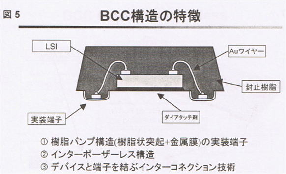
Main Features of BCC (Bump Chip Carrier)
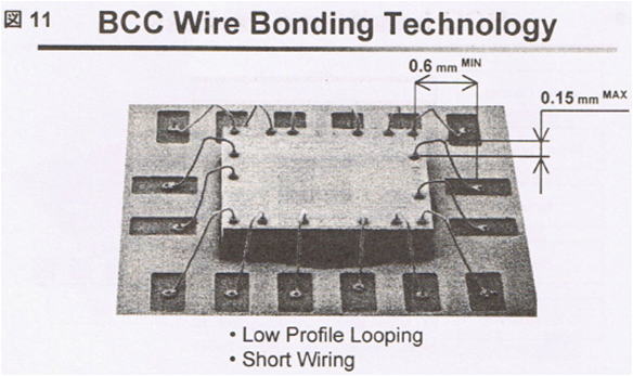
BCC Wire Bonding Technology
1997: Mass production of QFNs starts
Matsushita Electronics started mass production of a QFN (quad flat non-lead) package, which has a lead frame and is formed in a single-sided mold. The pins for connection are on the under-surface of the package.
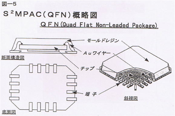
QFN (Quad Flat Non-Leaded Package)
1998: Mass production of stacked CSPs starts
Sharp started mass production of stacked CSPs. Multiple memory devices such as SRAM and flash memory were stacked in these stacked devices. Sharp also cooperatively developed stacked CSPs with Mitsubishi Electric Corporation. Fujitsu, NEC Corporation, and Toshiba Corporation announced similar structures in the same year. The race to develop stacked CSPs containing stacked memory devices in an MCP (multi-chip package) started. The approach of mounting multiple LSI-device layers in a single package began to be called the SiP (system in package) around this time, and the development of system LSIs using the SiP method started.
Stacked CSP
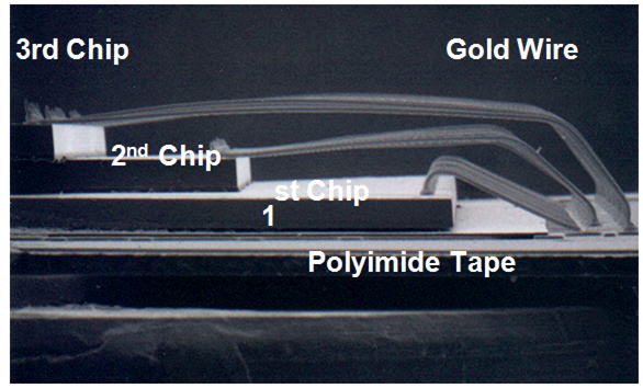
Wire Bonding of Stacked CSP
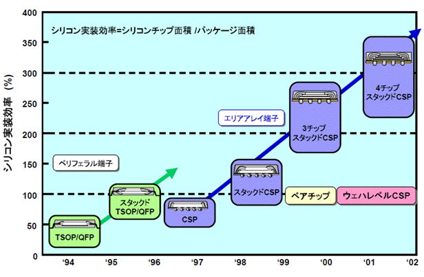
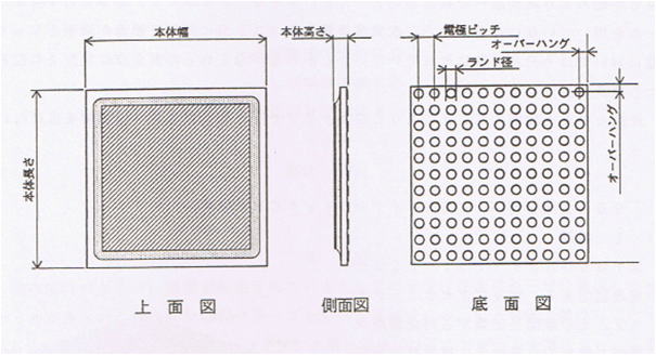
Advancement of Mounting EfficiencySilicon Mounting Efficiency = Silicon Die Area/Package Area
1998: Development of the COF for driving FPD screens
In 1998, Hitachi Cable, Ltd. proposed the COF (chip on film) structure in which the LSI devices for driving a flat display panel (FPD) such as a liquid crystal display are flip-chip connected to TAB tape. Omitting the finger leads that had been used before, the COF allowed further reductions in the bump pitches of LSI devices, and increased numbers of pins and improved production yields came to be consistently realized.
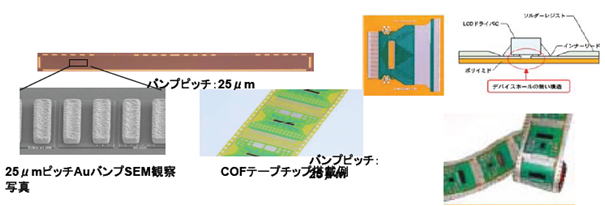
COF (Chip on Film) Structure
1998: Foundation of the Japan Institute of Electronics Packaging
The Japan Institute of Electronics Packaging (JIEP) was founded as a scholarly body to concentrate on packaging and related techniques. Its parent organizations included the Institute of Printed-Circuit Board Processing (formed from institutes concerned with printed-circuit boards). The JIEP also publishes a journal, and its formation led to an increase in the number of research papers from universities covering techniques for joints, materials, simulation, and so on in the semiconductor field.
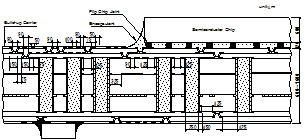
1998: Development of the WL-CSP formed on wafers
The merging of wafer fabrication processing and packaging technologies started and has been advancing. Development of the WL-CSP (wafer-level chip-scale package) was one such example. For this package, the section for joining to the printed-circuit board is created on the wafer after wafer processing steps by using plating interconnect technique, such as copper plating. Packaging process together with the wafer processing lowers the overall cost, and it was applied to low-pin-count analog ICs for mobile phones.
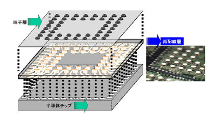
WL-CSP (Wafer Level Chip Scale Package)
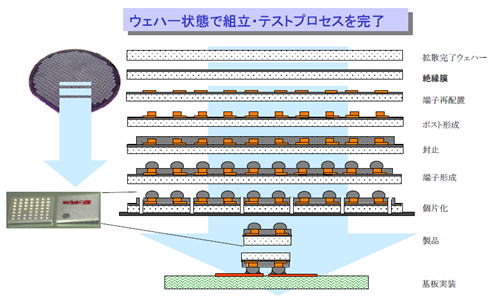
Manufacturing Process of WL-CSP
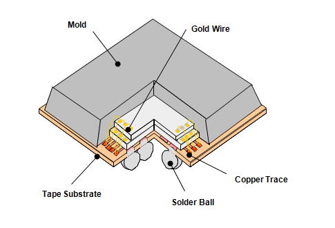
1999: Mass production of μBGAs for high-speed memory starts
After acquiring the technology of μBGA (R) structure as developed by Tessera, Inc. in the U.S., Hitachi Cable and Hitachi Ltd., worked together to review the structure, manufacturing process, and equipment. They then developed an original method for connecting gold-plated copper leads made on TAB tape to the aluminum electrodes of the LSI circuit, a technique to adopt adhesive tape with minute holes as a stress-absorbing film, and a technique for continuous transfer molding. They then started mass-producing CSPs in a reel-to-reel production system.
Package for 72-Mb Direct Rambus Memory
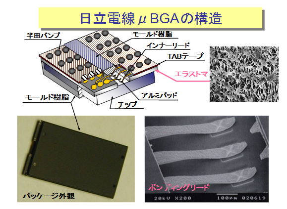
Structure of BGA from Hitachi Cable, Co. Ltd.,
1999: Start of the electronic SI project (ASET)
An electronic SI (systems integration) research project for the study of high-density three-dimensional stacked mounting was set up at the Association of Super-Advanced Electronics Technologies (ASET) as a national project of five year program (1999 to 2003). This project made a prototype of a CCD with a TSV (through-silicon via) structure in which through holes were opened in the silicon substrate and copper-plated pins for soldering were placed on both faces of the devices. Sanyo Electric Co., Ltd. completed a TSV structure in which the solder bumps were formed on the under-surface of the CCD device.