
Packaging Technology
Changes in Package Shapes of ICs and LSI devices
1970s
1970s: Era of pin-insertion dual in-line packages (DIPs)ICs and large scale integrated (LSI) circuits for calculators were the driving force for semiconductor packaging technology, so the industry in Japan was ahead of its counterpart in the U.S. in expediting packages with larger numbers of pins. Although hermetically-sealed packages preceded other types of package in the early 1970s, a plastic-sealed package that could be made at low cost was developed to support the expanding mass production of consumer electronics such as color TV sets. Design, production, material, and equipment techniques for plastic packages were widely developed and expanded in Japan in order to cope with the increasing number of pins in ICs, including LSI circuits, for calculators and the generally expanding production of ICs.
1970: Development of pin-insertion laminated ceramic packages
In the surface mounting of components, a soldering iron is used to solder ICs to the printed-circuit boards. A pin-insertion type was thus developed to further streamline the soldering process. Here, holes are drilled in a 100-mil grid pattern and the lead pins of the package are inserted in the holes. A package where the lead pins are arranged in two rows separated by 100 mil is called a dual in-line package (DIP). Distances between the rows of lead pins for 16- and 24-pin packages were 300 and 600 mil, respectively. Numbers of pins subsequently increased to 28, then to 40, and successively to 42 and 64. The pin-grid array (PGA) style where the pins are arranged in a grid pattern was adopted for packages with 52 and more pins.
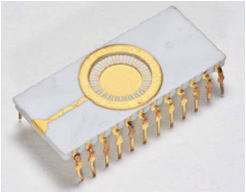
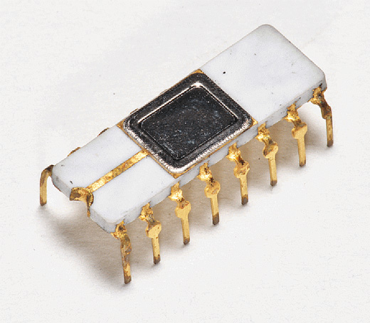
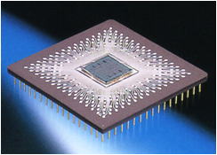
DIP Type Ceramic Package
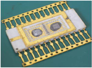
Die Mount in DIP Type Ceramic Package
1970: Expanded mass production of pin-insertion low-melting-point glass packages
The low-melting-point glass package was developed as a cheaper alternative to the laminated ceramic package. Low-melting-point glass materials were improved to increase reliability in terms of robustness against heat even in large form factors. These materials thus became applicable to the MOS-logic ICs and LSI circuits of, for example, large-scale computers and calculators. The low-melting-point glass package was referred to as CERDIP (ceramic DIP) or DILG (dual in-line glass package). Applicability of this was limited to packages with up to about 600 mil between the two rows of leads and up to about 28 pins. However, these were replaced by a cheaper resin-mold PDIP (plastic dual in-line package) as its reliability improved.
Packaging process flow
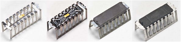
Early 1970s: Evolution of resin-mold DIL packages
Resin-mold packages were developed next as a cheaper replacement of hermetically sealed package than low-melting-point glass packages. Resin-mold packages were developed one after another. Firstly, 8-, 14-, and 16-pin resin-mold PDIPs, which were easy to mass produce, were developed for components of color TV sets. SILPs (single in-line plastic) with heatsinks for use in audio ICs followed this. After that, 40- and 42-pin epoxy-resin-mold packages for the LSI circuits of desktop calculators with 12- to 18-digit displays appeared. Silver paste replaced gold–silicon die bonds, and partial gold plating was developed into the sparger plating method of partially spraying the silver plating solution. Packages of this type had up to 64 pins in rows separated by 900 mil. For greater numbers of pins, resin pin-grid arrays (PGAs) were used instead.
Various Resin Mold DIL Type Packages
1971: Development of 36-pin packages for the Super High-Speed Computer Project
The Super High-Speed Computer Project was set up by the Japanese government with several aims, one being the development of domestically-produced ICs. A 36-pin package was developed for LSI circuits to be used by the association. Dual wiring layers were formed on an alumina-glazed alumina substrate, and sets of ten ICs were flip-chip interconnected to form LSI circuits. Lead pins were placed on all four sides of the package and seam welding was applied to the respective pairs of edges in the X and Y directions, after which the lead frame was bent by 90 degrees.
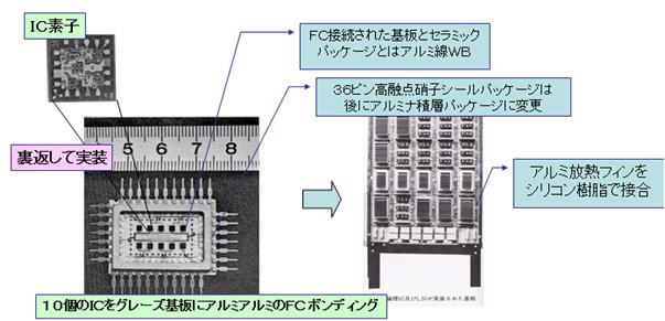
36-pin Package for Super High Speed Computer and the Board Mounting
1973: Development of automatic wire bonders for transistors
Hitachi, Ltd. developed automatic wire bonders for transistors. These machines take in the locations of the bonding pads of the transistor devices and the bonding positions on the lead frame as camera images and perform time-sharing pattern control accordingly. This image recognition system was widely adopted in the fabrication of ICs, including LSI circuits, and in industrial robots. This provided one basis for Japan later leading the world in the fields of semiconductor production and industrial robotics.
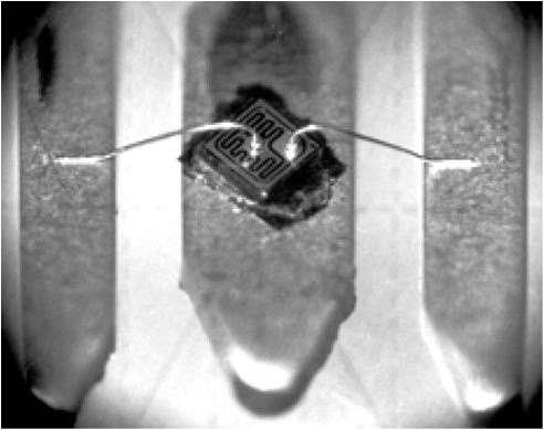
Photo after Wire Bond
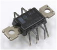
1973: Development of side-brazed packages
The side-brazed DILC was developed as a package with the lead frame silver-brazed to the side surfaces of the package body. This allowed the mounting of memory devices larger than can be accommodated by a standard DILC (DIL-type laminated ceramic package with rows of pins separated by 300 mil). As the scale of mass production increased, handling of the laminated ceramic technology was consigned to ceramics manufacturers (such as the Kyocera Corporation). Use of such packages subsequently expanded, for example, LSI circuits for microcontrollers in the U.S.
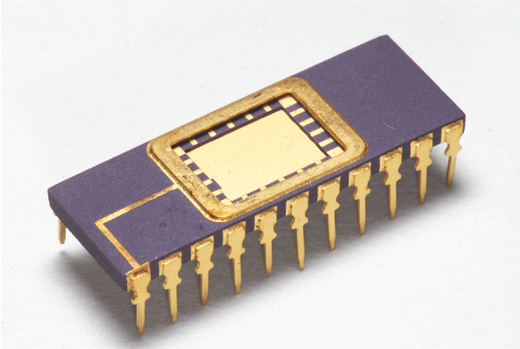
Side-brazed Ceramic DIP
Around 1975: Establishment of automatic dicing using a thin grinding wheel
The first automatic dicing machine was exhibited at Semicon West. To prevent damage to the MOS-IC gates due to electrostatic discharge in the pure water used for cooling in the dicing process, Hitachi developed the technique of adding carbon dioxide bubbles to the water. The Nitto Denko Corporation developed a tape that holds the devices in place after dicing and facilitates their separation in the die-bonding process.
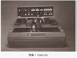
DAD-2H - Automatic Dicing Machine from Disco (then Daiichi-Seito)
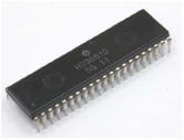
1975: Development of the PGA (world's first)
In response to the demand for small packages with large numbers of pins that accompanied the increasing scales of LSI systems, the 52-pin PGA (pin grid array) was developed by using a laminated ceramic technology in which the pins are arranged in a grid pattern. The lead pins are silver-brazed to holes opened on the ceramic substrate. This package was used in the ECLHD10K-series mainframe computers. The PGA's structure, with the lead pins placed in a grid pattern, facilitates support for relatively large numbers of pins, which subsequently increased to 72, then 100, and then even larger numbers of pins.
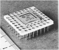
First 52-pin PGA
Advanced PGA Package with Large Number of Pins
1976: TAB technology applied to LSI circuits for calculators
The Sharp Corporation was the first to adopt tape automated bonding (TAB) technology for LSI circuits, specifically those for use with liquid crystal displays. The TAB technology enabled gang bonding and so was expected to reduce joining times relative to those for wire bonding. Shindo Co., Ltd. developed a method where sprockets or device holes are opened in the polyimide films used in TAB, glue is used to paste copper foil in the holes to form a three-layer structure, and the device holes are filled with resin before photographic exposure and processing.
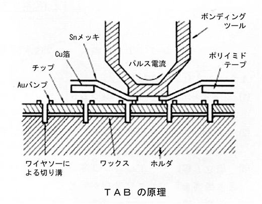
Basic Mechanism of TAB (Tape Automated Bonding)
Around 1977: Development of packages for EPROM
Each EPROM has a floating gate formed under the gate of the memory cell. This allows the electrons on the floating gate to be discharged to delete data in response to ultraviolet irradiation from outside the package. Packages with ultraviolet-transmitting glass were developed accordingly. Sapphire substrates and other materials were used for the ultraviolet-transmitting glass.
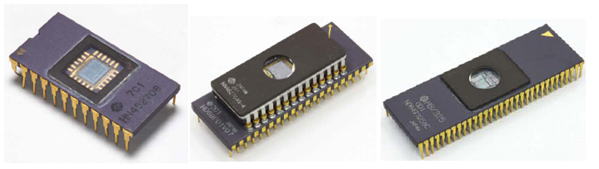
Packages for EPROM with UV-light Windows
1977: Birth of world's first QFP
MOS LSI circuits for calculators were requiring ever more pins because of the increasing numbers of digits being handled and the necessity of displaying characters in special ways in, for example, exponential functions. To satisfy this demand, the 54-pin quad flat package (QFP) for surface mounting was developed. Surface mounting made for a thin (thickness: 2.0 mm) package, which contributed to calculators becoming more compact and slimmer. The thickness of the lead frame was 125 μm but the length of the lead pins was 1.7 mm because manual soldering was still required. This package type was used for the LSI circuits of desktop calculators with displays handling large numbers of digits, and for 4-bit microcontrollers. The initial name for the package was FPP (flat plastic package), but this was changed to QFP (quad flat package) after discussion at the Technical Standardization Committee on Semiconductor Device Package.
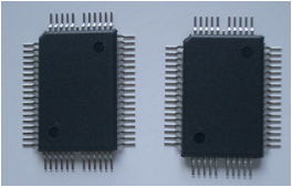
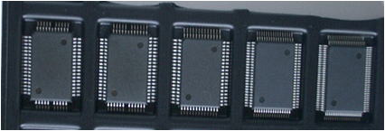
QFP (Quad Flat Package)
1979: Development of solid-state image-sensing devices
As VCRs became widely used, a laminated ceramic package with transparent glass was developed for use with solid-state image sensing devices for image capture in consumer camcorders. After that, many advanced forms of packages were developed for devices that capture images, such as CMOS sensors and CCDs, including line sensors to read the light from light-emitting diodes (LED) in OA and FA applications.
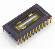
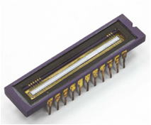
Ceramic Package for Image Sensors