
Packaging Technology
Changes in Package Shapes of ICs and LSI devices
1960s
1960s: Era of TOP (transistor outline packages)The 1960s were the early days of the integrated circuit (IC). IC technology was introduced from the U.S. semiconductor companies then packaging materials and technologies of assembly equipment were subsequently developed by various Japanese companies. As the quantity of ICs continued to increase from the late 1960s, technologies for materials and for equipment used in semiconductor packaging started to be consigned to specialized manufacturers. Fabrication technology was, so to speak, transferred to specialized manufacturers.
Around 1960: Can-type packages for transistors
Packages for transistors were developed on the basis of packages for vacuum tubes. High-melting-point glass is used to weld the terminal area to a metal base. This glass component is called the stem. Separate leads are soldered to each pin of an alloy transistor and a metal cap plated with tin is placed over this. Interdigitated sealing is performed for the stem and metal cap by the tin-tin joint.
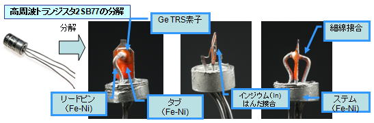
Dismantlement of High-Frequency Transistor 2SB77
Around 1964: Development of micromodules
A micromodule is a compact and high-density three-dimensional layered package realized by forming printed thick-film resistors and capacitors on alumina ceramic substrates produced through a dry-forming process and with metalized edge faces, bonding transistors to the substrates, piling multiple substrates on top of one another, and using solder to join the edges via metal leads. One field of application was helmet-mounted wireless equipment.

Micromodules - Products and Structures
Around 1965: Birth of MOS transistors
Transistor devices came to be mounted in four-pin can-type packages once the crystal face of Miller index <100> was found to have the best characteristics as a silicon crystal face for metal-oxide semiconductor (MOS) transistors. Such transistors became the basic elements of MOS LSI circuits, and afterwards evolved into n-channel metal oxide semiconductor (nMOS), complementary metal-oxide semiconductor (CMOS), etc.
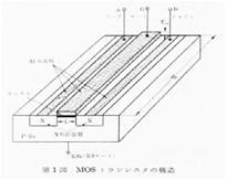
Structure of MOS Transistor

Aspecification of Transistor
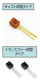
Around 1965: Development of resin-mold packages
Mass-production in increasing quantities led to the development of resin-mold packages, which use cheaper materials than can-type packages. The tip of a metal wire (called the lead) with a diameter of approximately 0.4 mm is flattened in a press, and three such leads are affixed to a jig. After the flattened sections have been joined by die bonding and gold wire bonding to the transistor chip, the result is placed in a concave jig. Silicon resin is then poured into the concave portion and heated. The package is completed once this has dried to become rigid.
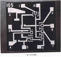
Linear ICs for Color TV - 10 ICs were used for Hitachi Color TV ("Pompa")
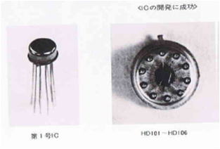
1966: Completion of Hitachi's first IC
The ICs, each approximately 1.2-mm square, were formed on a one-inch wafer. The package was a 10-pin can-type TOP and the chips contained basic logic circuits such as AND and NOR gates.
Chip Pattern of First IC from Hitachi
First IC Product
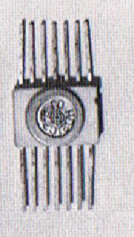
1967: Development of diode transistor logic (DTL) in 10-pin FPG packages
Since the number of lead pins in ICs continued to increase, the flat package glass (FPG) method for making small packages with many leads was used to develop a surface-mount package that had 10 pins. Metal leads were produced by etching a thin sheet and the result was called a lead frame. Aluminum was deposited on the tip sections of the lead frame by vapor deposition, and ICs were connected by ultrasonic bonding with aluminum wires.
DTL IC in FPG Package
Die Photo of DTL IC after AL Interconnect
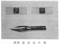
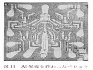
1968: Full-scale development of hybrid ICs
A technique was developed for forming ICs by screen printing thick-film resistors and capacitors on an alumina ceramic substrate and then connecting devices such as transistors and diodes on the same substrate. Such ICs are called hybrid ICs and used in the power supplies of TV sets and regulators of automobiles.
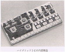
Internal Structure of Hybrid IC
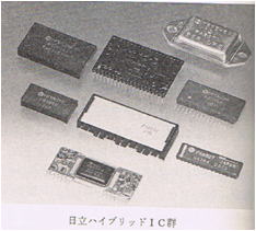
Hybrid IC Products from Hitachi
1968: Birth of Japan's first laminated ceramic package
A hermetically-sealed package offering high reliability in terms of robustness against heat and capable of handling the constantly increasing numbers of IC pins became necessary. Laminated ceramic package technology from the RCA Corporation was introduced in response, and the 14-pin FPC (flat package ceramic) was developed from this.
14-pin FPC (Flat Package Ceramic)
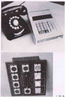
1969: Development of 42-pin FPC packages
A 42-pin laminated ceramic package for surface mounting was developed. This made it possible to produce a desktop electronic calculator from ten MOS-ICs mounted in the same package.
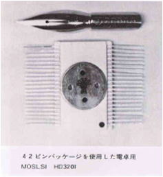
HD3201 - MOSLSI for Calculator in 42-pin Laminated Ceramic Package
Calculator using MOSLSIs and its LSI-Mounted Board