Equipment & Material
1980’s
Collaborative development activities between device manufacturers and equipment/material suppliers had become more active as the device miniaturization entered into in the submicron region. Antitrust law was revised and SEMATEC, modeled after the VLSI Technology Research Association in Japan, was established in the U.S. It became common understanding that manufacturing equipment and materials were the common base of the semiconductor industry. More than 80% of the world's semiconductor manufacturing equipment and materials were then supplied from Japan and the United States.
1980s: g-line stepper(reduction-projection exposure system)
The g-line stepper, which had started with a reduction ratio of 10:1, achieved a reduction ratio of 5:1 significantly improving productivity in 1982. The subsequent development of higher N.A. (Numerical Aperture) improved resolution. And the g-line stepper has entered the era of full-scale reduction- projection exposer systems.

1980s: g-line resist
Photoresists which was available for g-line photolithography were developed in 1979s, and the g-line reduction- projection exposure method was widely used in the 1980s.
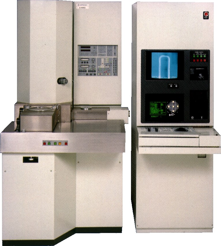
1984:Critical Dimension-Scanning Electron Microscope(CD-SEM)
CD-SEM which was a system used in the manufacturing lines for measuring the dimensions of fine patterns utilizing a scanning electron microscope (SEM) was developed to replace the optical systems in 1984. This enabled high-precision dimension measurement of fine patterns fabricated by lithography which was challenging to overcome optical limits.
1985: SEAJ was established
The Semiconductor Equipment Association of Japan (SEAJ) was established in 1985.
1986: Vertical furnaces
As wafer processes proceeded to submicron region, horizontal furnaces used for oxidation, annealing, LP-CVD, and other processes were replaced by vertical furnaces. The productivity had been improved through improved film deposition uniformity and reduced micro-particles contamination, as well as a smaller footprint, automated handling of wafers, and less frequent replacement of quartz components.
Late 1980s: High-density plasma-ion source single-wafer etching system
In the frond-end process of semiconductor manufacturing, the batch processing equipment which processed multiple wafers together was the main for cleaning, diffusion, film formation, and etching except for exposure of a mask pattern on a wafer. In the latter half of the 1980s, single-wafer etching equipment using high-density plasma ion sources which increased etching speed, became mainstream.
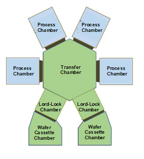
Late 1980s: Single wafer cluster tools
In front-end process of semiconductor, the manufacturing process such as cleaning, diffusion, deposition, and etching except for mask patter exposure on wafers had been mainly performed by batch processing equipment which collectively processes a plurality of wafers. Etching systems were first converted to single-wafer systems in the late 1980s, and then some deposition processes were also converted to single-wafer systems. Along with the shift of these processes to single-wafer systems, the modularization of process chambers progressed, and multi-chamber cluster tools had widely used aiming at the continuous processing of multiple processes and the improvement in productivity.
1987: SEMATECH semiconductor manufacturing equipment development
SEMATECH which was established in 1987 in the U.S. focused on the development of semiconductor manufacturing equipment. As a result, manufacturing equipment and materials became technology platforms for device manufacturing company. Since the 1990s, the U.S. semiconductor industry had shifted to a business model that device companies pursued in a differentiation with their product concepts and specification, which opened up a variety of new semiconductor applications.
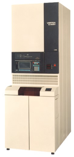
1988: Coater/developer
The coater/developer used in the photoresist coating/developing process was developed in 1988 with a multi-stage processing chamber configuration and a robot arm in order to transport wafers, resulting in high throughput and space savings.
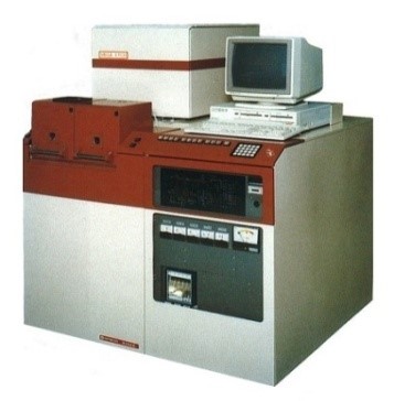
1988: Tungsten CVD System
The W (Tungsten)-CVD equipment forming the W plug which became an important part of VLSI process in submicron region appeared.
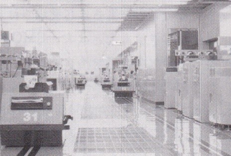
Late 1980s: Fully automatic fab
Mitsubishi Electric realized the first fully automated fab at its Saijo Works by using robots, overhead transportation system and FA system in 1984. Afterwards, the SEMI standard was established and this standard spread all over the world.