
Discrete Semiconductor Devices, etc.
2020s
2020 : Release of 1/2-inch SXGA InGaAs-Si- stacked visible and short-wavelength infrared light image sensors (Sony)
Sony released a small (1/2-inch) image sensor capable of imaging visible and short-wavelength infrared light (wavelength: 0.4-1.7μm) in May 2020. A back-illuminated InGaAs photodiode array chip (1280x1024 pixels, 5μm pitch) was stacked on a Si CMOS readout circuit chip. The electrodes between the chips were connected by Cu-Cu direct bonding.
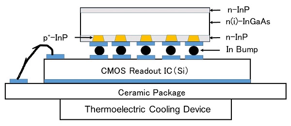
Schematic of the cross-sectional structure
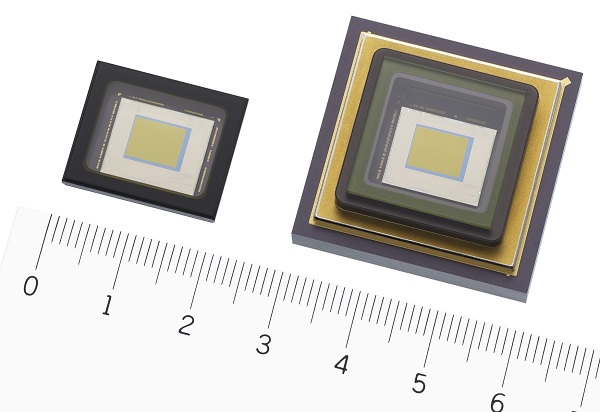
SWIR image sensor (IMX990)
Example of imaging
2021 : Development of 10W-class high-power blue semiconductor laser diode (Nichia)
Nichia has developed a high-power GaN-based semiconductor blue laser diode that emits 11.2 W of blue light (wavelength: 455 nm), the world's highest optical output per emitter stripe.
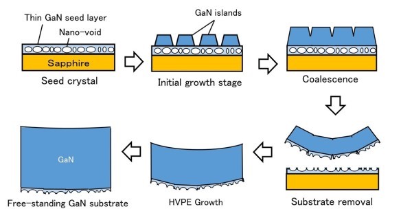
Fabrication process of free-standing GaN single-crystal substrates

Free-standing GaN single-crystal substrates
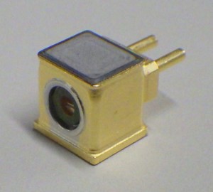
High output blue LD
2022 : Development of terahertz device using resonant tunnel diode (RTD) (Canon)
Canon has developed a terahertz wave oscillating device with an output power of approximately 12 mW at a frequency of 450 GH by monolithically integrating 6x6(36) double-resonant-tunneling-diode patch-antennas and synchronously operating all antennas.
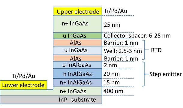
Cross-sectional structure of a resonant tunnel diode
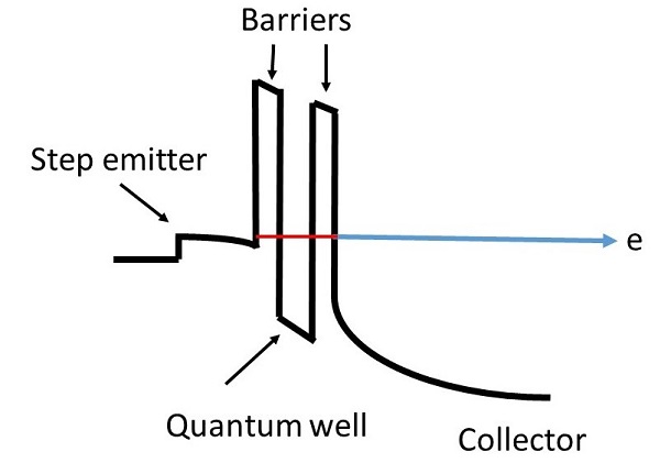
RTD band structure
RTD-based THz source
2022 : Launch of SPAD direct ToF method depth sensor for automotive LiDAR (Sony)
Sony launched a SPAD(Single Photon Avalanche Diode)direct ToF (Direct Time of Flight) method depth sensor for automotive LiDAR (Light Detection and Ranging), in which a back-illuminated SPAD pixel chip and a logic chip integrating signal processing circuits were stacked with Cu-Cu (copper-copper) connection. Micro-lenses and concavo-convexities on the light input surface increased the incident light absorption, achieving a high Photon Detective Efficiency (PDE) of 24% for light at wavelength of 905nm. It enabled high-speed, high-precision distance measurement with resolutions of 15cm from distance of 200m to close range.
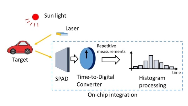
Schematic of LiDAR system
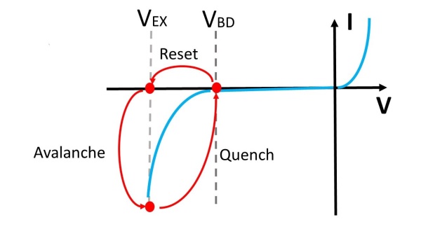
I-V characteristics of SPAD and photon counting operation
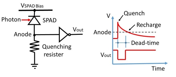
SPAD Photodetector circuit and operating waveforms
2023 : Development of a wider-temperature-range 100 Gbps Electro-absorption Modulator integrated Laser (EML) for data centers (Mitsubishi Electric)
Mitsubishi Electric has developed an Electro-absorption Modulator integrated Laser (EML) operating at communication speed of 100 Gbps over a wide chip temperature range between 5℃ and 85℃. 400 Gbps optical transceivers for data centers can be realized by four-wavelength multiplexing without temperature control TEC.
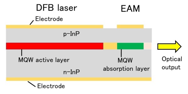
Schematic of the structure of EML
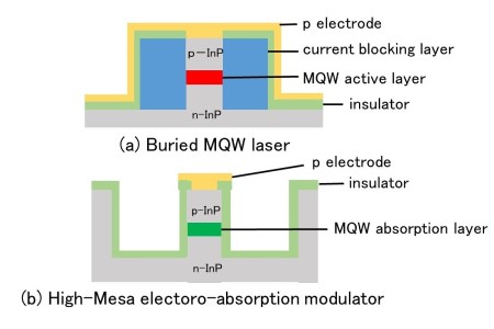
Cross-sectional structure of EML element
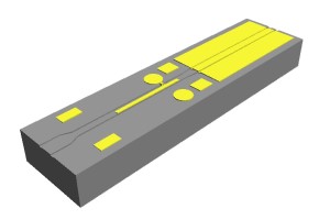
Electro-absorption Modulator integrated Laser (EML)