
Discrete Semiconductor Devices, etc.
2000s
2000: Development of a 4.5-kV 1.5-kA injection-enhanced gate transistor (IEGT) (Toshiba)
Toshiba improved the trench-type IGBT to increase the amount of electron injection on the emitter side and achieved a high breakdown voltage and low on-state voltage in July 2000. This development enabled the replacement of conventional gate turn-off thyristors (GTO) with IEGTs in fields of application in which GTOs had been in use.
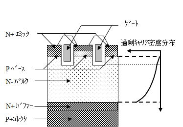
Structure of Trench IGBT

Structure of IEGT
2002: Release of a 10-Gbps surface-emitting semiconductor laser (Fuji Xerox Co., Ltd.)
The surface-emitting laser was proposed by Kenichi Iga of Tokyo Institute of Technology in 1977 and its continuous operation at room temperature was demonstrated for red emission in 1988 and for emission at 1.3 μm in 1993. However, the complexity of the fabrication process meant that practical applications were slow to come.
In June 2002, Fuji Xerox released a commercial laser for 4-mW output at 850 nm to support 10-Gbit Ethernet communications. This laser was suitable for driving transmission over plastic optical fiber.
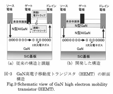
2003: Development of a gallium-nitride HEMT for W-CDMA base stations (Fujitsu)
Strong expectations were held for gallium-nitride-based semiconductor materials in terms of realizing transistors capable of high-temperature operation, high breakdown voltages, and large output. The HEMT structure improves electron mobility, allowing operation in the high-frequency range. The development of power transistors of this type to drive motors and for use in power-supply circuits is still proceeding.

March 2003: Development of a large-output blue-violet laser (Sanyo Electric Co., Ltd.)
The standard for the large-capacity Blu-ray optical disk was defined in February 2002, and manufacturers proceeded to develop a laser for it. Sanyo led by developing the first large-output gallium-nitride-based laser, which was able to output 100-mW pulsed light at 405 nm.

Schematic Cross Section of Blue-Violet Laser with Carrier Block Layer
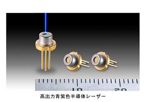
Large output blue-violet semiconductor laser
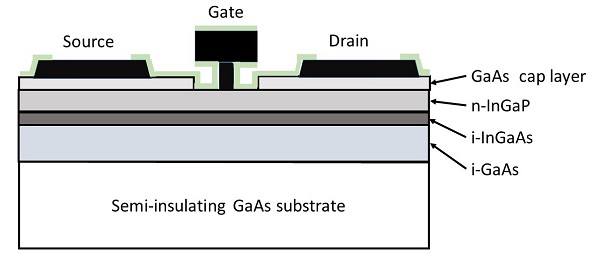
2004: Development of InGaP/InGaAs HEMT MMIC for 76GHz automotive radar
Fujitsu developed InGaP/InGaAs HEMT MMIC (Microwave Monolithic Integrated Circuits) technologies for 76GHz automotive radars. Fujitsu TEN's world's first forward looking millimeter-wave radar using this technology was installed in the Toyota Crown MAJESTA.
InGaP/InGaAs HEMT cross sectional structure

Photograph of single chip integrated MMIC

3D-scan 76GHz automotive radar
2006: First delivery of 100-lm/W white LED samples (Nichia)
A diode capable of emitting white light was proposed in 1966. This was composed of a phosphor that emits yellow light with a high luminosity and a blue light-emitting diode. Through the improvement of blue light emitting diodes, Nichia was able to start delivery of 100-lm/W white LED samples in June 2006. These devices provide comparable brightness to that of a fluorescent light. Nichia now has a 60% share of the world’s production of white LED chips.
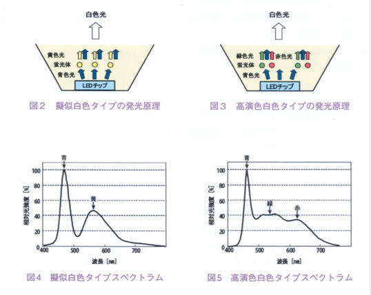
Luminescent Principle and Spectrum of White LED
2007: World's first OLED TV launched (Sony)
Organic Light-Emitting Diode (OLED) displays are superior to Liquid Crystal Displays (LCDs) in terms of self-luminescence, fast response, thin plate, low voltage drive, and high contrast.
OLED displays had been used in automotive displays and displays for mobile devices. Sony was the first company in the world to launch an 11V-type OLED TV,"XEL-1" on December 1, 2007, spearheading the use of OLED displays in TV applications.

Cross-sectional structure of 'Top-Emission' OLED display

The world's first OLED TV, 'XEL-1'
2008: Development of a full-frame 35-mm 24.18-million-pixel CMOS image sensor (Sony)
Due to their ease of monolithic integration with CMOS logic circuits, CMOS image sensors were first used in small and low-cost applications such as mobile phones. As technologies to reduce pattern noise and switching noise were developed, however, large-image sensors that took advantage of the low power consumption and fast operating characteristics of CMOS image sensors were developed and applied in digital single-lens reflex cameras.
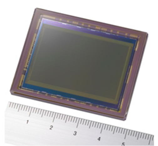
Photo of Full-Frame 35-mm CMOS Image Sensor
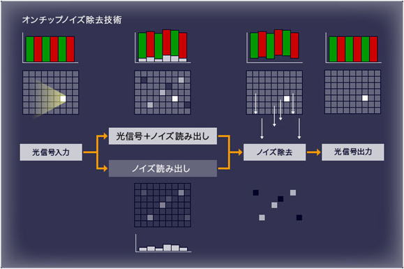
On-Chip Noise Rejection Technique to Remove Fixed Pattern Noise
2009: Start of mass-production of world’s first 1310-nm quantum-dot laser for 10-Gbps communications (QDLaser)
The quantum-dot laser was proposed by Yasuhiko Arakawa and Hiroyuki Sakaki of the University of Tokyo in 1982 and its operation was confirmed in 1994. A quantum-dot laser is less affected by changes in temperature than a conventional semiconductor laser and provides stable operation at up to 100°C without requiring complicated temperature control. As quantum dot-fabrication technology advanced, the world’s first commercial quantum-dot laser with a wavelength of 1310 nm for 10-Gbps communications was released in March 2009.
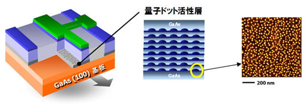
Schematic Cross-Sectional View of Quantum-Dot Laser