
Japanese Pioneers
Hideo Inuzuka
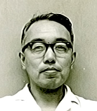
Hideo Inuzuka was born in 1910. He went to work for Tokyo Shibaura Electric Co., Ltd. in 1936. He became the manager of the Semiconductor Materials Research Department at the Central Research Laboratory of the same company in 1961 and deputy director at the laboratory in 1965, while also working as an assistant to the general manager of the transistor factory. He was made an executive (as assistant manager of Central Research Laboratory) in 1968.
Having been interested in minerals for use in mineral detectors since his junior high school days, Inuzuka studied crystal structures in the mineralogy department at the School of Science at Tokyo Imperial University. He entered Tokyo Shibaura Electric Co., Ltd in the middle of his graduate school days. After research into silica glass and titanium-oxide ceramics at the Matsuda Laboratory, he began to be involved in artificial crystals after refining silicon crystals for radar detectors during Second World War. As germanium was focused on, his earlier studies made him a central figure both inside and outside the company. With early success in the floating-zone melting of single-crystal silicon, he laid the foundation for the mass production of best-of-their-class high-voltage large-current rectifying elements from 1967. In 1958, he started a transistor factory called the Theatre Toshiba with its first general manager. With a focus on the environment, this factory covered the entire manufacturing process from raw materials to finished products. This factory laid the foundation for Toshiba becoming the predominant player in world-wide production of germanium transistors in later years. In 1962, he became the first to succeed in making synthetic diamonds in Japan. The existing way of synthesizing diamonds required very high voltages and temperatures, so this work was a big step towards commercialization, because the introduction of a newly developed catalyst roughly halved the required voltage and temperature relative to the existing method from GE.
He also played a leading role in developing technologies to produce and evaluate crystalline materials in general, including work at Toshiba’s Central Research Laboratory on ferrite single crystals, single crystals of compound semiconductors, and in further products development through the application of these technologies.