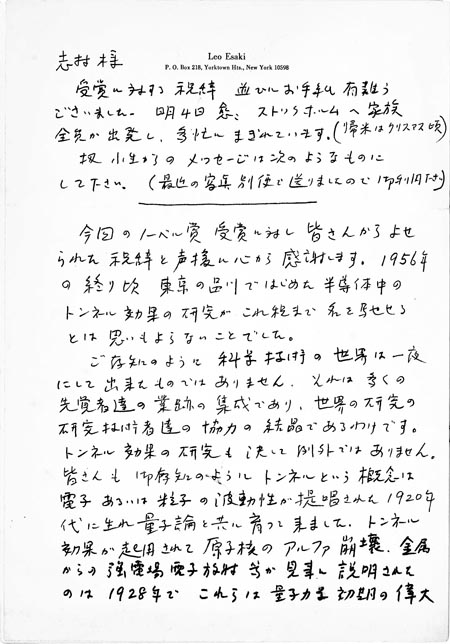
5) Creating a Superlattice the Night Before the Big News

Esaki’s thank-you note for the special edition of “Electronic Materials” (Click
to enlarge)
The picture above is Esaki's thank-you note for the special
edition of "Electronic Materials" to congratulate him on winning the Nobel
Prize.
Written at the top, "I will be in Stockholm for the awards ceremony tomorrow,
December 8th", was done in the middle of his now extremely busy schedule.
Even so, reading the packed 5-page letter, it is possible to feel the depth
of Esaki's thoughtfulness and sincerity.
What interested me in this letter was that he happened to be working late
into the night on a semiconductor superlattice experiment with his colleague,
the night before the award would be decided. We had just succeeded in making
a 100Å period superlattice for the first time with a combination of gallium
arsenide and aluminum gallium arsenide.
At the end of the letter, he added, "Although it is common sense to tell a
story of your past in the Nobel Prize commemorative lecture, I decided to
include my new experiment results from the current period of awarding the
prize in addition to my past work. There will be some people who will laugh
that it is Esaki’s way…”