28) Argument over Ion Implantation

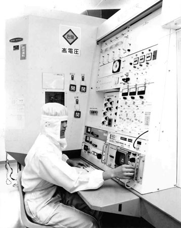
Ion implantation equipment in Hitachi’s 64K-bit DRAM production line
As the capacity of DRAMs increased, ultra-expensive manufacturing equipment
such as ion implantation equipment was introduced in semiconductor factories.
The photograph is from Hitachi's 64K-bit DRAM production line in the early
1980s.
Ion implantation systems gained a high profile in Japan since JDRC(Research
Development Corporation of Japan) chose and focused on ion implantation technology
as a major challenge in 1968. Two groups - Susumu Namba, a senior researcher
at RIKEN and also a processor at Osaka University teamed with Hitachi, and
Tadatsugu Ito, a processor at Waseda University with Toshiba - were organized
and they intensively conducted research and development toward practical application.
This is the story behind the devolvement of ion implantation technology in
Japan.
In a story from Namba, when he made a presentation on the situation of Ion
implantation technology development in US at the 132nd Committee of JSPS (Japan
Society for the Promotion of Science), "Application of Charged Beams
in Industrial Science" , there came out many negative arguments such
as "large ions cannot enter deep into the crystal," and “if they
do enter, the crystal will be destroyed and the technology can never serve
for practical use. "
Later, Namba and I were invited and visited Taiwan. When discussing on the
future of nanotechnology in Taiwan , professor Namba said "In the beginning,
ten out of ten people were not in favor of implantation technology".
I still remember this comment made by him. (provided by Hitachi. Ltd.)
| To page top | To Part 2 index |