1) Kilby's Monolithic Idea in as short as Two Months

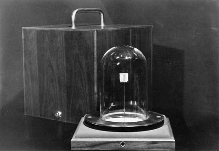
Picture A: Jack Kilby's integrated circuit (IC), displayed at the Tsukuba
Science Expo

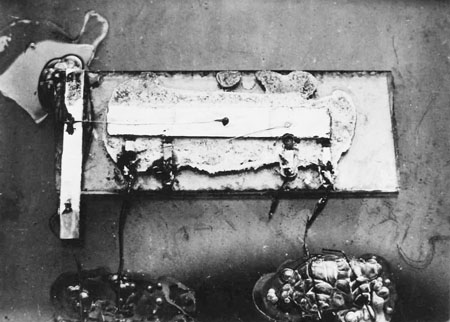
Picture B: A close-up view of the integrated circuit (Pictures provided by TI Japan)
“Of all of the developments of semiconductor industry in the
past quarter century, this one was truly exciting and dramatic; it exceeded
my expectations.”
In 1985, Jack Kilby came to Japan for the Tsukuba Science Expo, which included
an exhibit of the integrated circuit which he invented. Kilby was as tall
as 2m, surprisingly tall to my Japanese eyes. Kilby made some time to sit
down with me for an interview.
One of the interesting parts of the interview was that it took him only two
months period from the concept to the realization of his “Monolithic Idea,”
which was the concept of putting multiple components into a single semiconductor.
In May of 1958, Kilby left the electrical component maker Centralab to join
the up-and-comping transistor maker, Texas Instruments. As a newcomer not
eligible for vacation, he spent July alone in the factory hard at work on
his plans for integration.
Suddenly one day, the idea came to him that “...if all the components were
to be made from a single material, they would be internally connected, forming
a perfect circuit and we would be able to integrate everything.” This is what
would become the “Monolithic Idea." Kilby's first IC was a phase-shift
oscillator made with five integrated components on a 4mm by 9mm germanium
substrate. It was completed on September 12th, 1958.
Furthermore, 1959 brought the completion of the first operating flip-flop
circuit, and in March of the same year, it was given the name “Solid Circuit”
and displayed at the IRE Show (later to be called the IEEE Show).
| To page top | To Part 2 index |