Japan Semiconductor Innovation 50 (T-10 1980s)
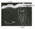
Three-Dimensional Cell Structure to DRAM (Hitachi)
Reduction of signal storage level along with the dimensional
scale down and capacity increase of DRAM raised fundamental problems of
unstable device operation such as "soft error". Various technologies
to solve the problems, such as "ONO gate-oxide" by NEC (1976),
were developed. And new three-dimensional cell structures were later invented
and developed to drastically increase the cell storage capacity which provided
a fundamental countermeasure to the problem.
"Stacked Capacitor Cell Structure" was presented at IEDM in 1978
by Koyanagi of Hitachi, and "Trench Cell Structure" was presented
also at IEDM in 1982 by Sunami of Hitachi. Both technologies were later
adopted in Mega-bit DRAM products and in the following generations and became
fundamental DRAM technologies.
| Cross Section of Stacked Cell | Cross Section of Trench Cell |
 |
 |
| (Reference 1) | (Reference 2) |
Remarks column
To main gallery (Process Technology 1980s)
Reference 1:
Technical Digest of IEEE International Electron Devices Meeting, pp.348-351,
1978.
Reference 2 :
Technical Digest of IEEE International Electron Devices Meeting, pp.806-808,
1982.