Japan Semiconductor Innovation 50 (T-8 1980s)
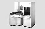
CD -Critical Dimension- SEM (Hitachi)
Hitachi developed CD-SEM, S-600, machine which marked an
epoch, with a novel idea of fine geometry measurements of semiconductor
devices using scanning electron microscopes. It specializes in measurement
function of SEM among various other functions. The machine offers automatic
measurement capability of pattern width of several hundred nm, and is applied
to the dimensional control in semiconductor front-end manufacturing processes.
Low acceleration voltages below 1kV are used in order to cope with non-conducting
sample materials, avoiding the damage on them. Pattern edges are automatically
detected, and standard magnification samples like standard micro-scales
are used to secure high precision measurement. Hitachi secured more than
80% market share according to the 2008 statistics.
CD-SEM "S-600" |
 |
| Quote from Hitachi Hyoron |