Japan Semiconductor Innovation 50 (D-8 1980s)
Advanced Technologies in DRAM
NEC succeeded in applying NMOS technology to 4K-bit DRAM,
µPD403, in 1971, while conventional DRAMs were in PMOS, and played
a leading role in realizing higher performance DRAM. Japanese semiconductor
companies realized higher quality and manufacturing yield and established
the leading position in the DRAM market from 16K DRAM generation, and further
increased their share of market in 64K generation in the early 80's and
thereafter.
Japanese manufacturers led the global industry in the advanced technologies
of DRAM, as well as their productization, including high reliability and
low cost plastic packages, high performance CMOS, multi-level interconnect,
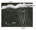
folded-bit line architecture to cope with lower signal levels, three-dimensional
memory cells such as stacked cells and trench cells. They led the progress
of semiconductor manufacturing technologies, as well as leading in world
semiconductor share.
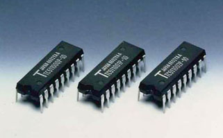
Toshiba 1M DRAM |
Cross Section of Stacked Cell | Cross Section of Trench Cell |
 |
 |
 |
| Offered by Toshiba | Photo reference 1 | Photo reference 2 |
Remarks
Photo reference 1
Technical Digest of IEEE International Electron Devices Meeting, pp.348-351,
1978.
Photo reference 2
Technical Digest of IEEE International Electron Devices Meeting, pp.806-808,
1982.