September 2011
I have tried to support the activities of Semiconductor
History Museum of Japan as an advisor from the very first stage, and I feel
very much honored that a special exhibition room carrying my name is now opened
in the Museum. I feel like becoming a mummy myself from a mummy-hunter.
Why Semiconductor History Museum now?
The semiconductor industry started right after the Second World War, and the
annual rings now count more than 60 since that time. Various events and products,
including their memories even during the developing period, needless to say
during the pioneering days, are now about to fade away in the history.
Actually, the technical documents and product samples are scattered and sometimes
completely lost in the course of repeated industry and factory restructuring.
Kusatao Nakamura, a poet who flourished through the early Showa era, wrote,
“The Meiji era is now an old, faded page of history,” and nowadays even “the
post war days” are already far away.
It is my great pleasure if this exhibition room serves to complement the hollowing-out
of technical documents in this kind of situation.
Japanese semiconductor industry started by learning from US, proactively accepting
their technology and manufacturing schemes, but it also played original and
creative roles in in the globalization of the industries in the milestones
of the time.
It is a grateful boon from the wisdom and efforts of predecessors that Japan
could become a semiconductor manufacturing country exceeding US even in a
limited period of time.
I was luckily involved in these historical scenes as a technical journalist
and could observe the events by my own eyes. I tried to delineate the birth
and development dramas of Japanese semiconductor industry, focusing on “People,”
“Companies” and “Technologies” by presenting the photos and technical documents
which I accumulated through my long work career. I also considered for the
readers so as to be able to grasp the overview of history by reading the whole
part. I ask the readers to allow my personal judgement and liking in some
parts, even though I tried to keep fairness and accuracy in selecting the
themes and descriptions as much as possible. I also would like to express
my gratitude to the supports of many people in providing the documents and
confirmation of facts.
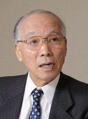
Yukio Shimura
Mr. Yukio Shimura’s brief personal history
He was born in Hokkaido in 1935, and graduated from Education Department
of Waseda University. He worked as an editor of the technical magazine “Densi-Zairyo
(Electronic Materials & Parts)”at Kogyo Chosakai Publishing Co., Ltd.
Afterwards, he became President and Chairman of the company.
During his career at the company, he served as a member of government-related
committee, Industrial Technology Council, and Officer at Gakkyoukai - The
Association of Japan Studies, including Board Chairman of Natural Science
Publication Society.
And also, he was in charge of lectures in advanced technology fields at
Science and Engineering Department of Waseda University, International Economics
Department of Reitaku University, and Economics Department of Nagoya University.
He currently lectures on Venture Business Studies at Common Educational
Organization of Kanazawa University.
He wrote more than 30 books and also newspaper serial publications which
are all excellent technology review and critique, including “Origin of Technology
Intensive Nation ― Japan,” “Half a Century of Japanese Semiconductor Industry,”
“’Japanese Way of Technology Thinking Conquering the World,” “Ig Nobel Prize
of Science Makes You Laugh,” “Unofficial History of Semiconductor Industry
– Half a Century of Innovation”
(*) Note: These are unfortunately all in Japanese language and not available
in English.
[To page top ]


